Product Summary
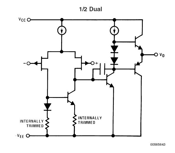
The LF412CN is a Low Offset, Low Drift Dual JFET Input Operational Amplifier with very low input offset voltage and guaranteed input offset voltage drift. The LF412CN requires low supply current yet maintain a large gain bandwidth product and fast slew rate. In addition, well matched high voltage JFET input devices provide very low input bias and offset currents. The LF412CN dual is pin compatible with the LM1558, allowing designers to immediately upgrade the overall performance of existing designs.
Parametrics
LF412CN absolute maximum ratings: (1)Supply Voltage: ±18V; (2)Differential Input Voltage: ±30V; (3)Input voltage Range (Note 3): ±15V; (4)Output Short Circuit Duration (Note 4): Continuous; (5)Power Dissipation: 670mW; (6)Tj max: 115℃; (7)θjA (Typical): 115℃/W; (8)Storage Temperature Range: -65℃≤TA≤150℃; (9)Lead Temp. (Soldering, 10 sec.): 260℃; (10)ESD Tolerance (Note 13): 1700V.
Features
LF412CN features: (1)Internally trimmed offset voltage: 1mV (max); (2)Input offset voltage drift: 10μV/℃ (max); (3)Low input bias current: 50pA; (4)Low input noise current: 0.01pA/√ ̄Hz; (5)Wide gain bandwidth: 3 MHz (min); (6)High slew rate: 10V/μs (min); (7)Low supply current: 1.8 mA/Amplifier; (8)High input impedance: 1012Ω; (9)Low total harmonic distortion ≤0.02%; (10)Low 1/f noise corner: 50 Hz; (11)Fast settling time to 0.01%: 2μs.
Diagrams

| Image | Part No | Mfg | Description |  |
Pricing (USD) |
Quantity | ||||||||||||
|---|---|---|---|---|---|---|---|---|---|---|---|---|---|---|---|---|---|---|
 |
 LF412CN |
 National Semiconductor (TI) |
 Operational Amplifiers - Op Amps |
 Data Sheet |

|
|
||||||||||||
 |
 LF412CN/NOPB |
 National Semiconductor (TI) |
 Operational Amplifiers - Op Amps LOW OFFSET,LOW DRIFT DUAL JFET INP OP AMP |
 Data Sheet |

|
|
||||||||||||
 (China (Mainland))


