Product Summary
The TDA3653B is a vertical deflection output circuit for drive of various deflection systems with currents up to 1.5 A peak-to-peak.
Parametrics
TDA3653B absolute maximum ratings: (1)Supply voltage (pin 9), VP = V9-4: 40 V; (2)Supply voltage output stage (pin 6), V6-4: 60 V; (3)Output voltage (pin 5), V5-4: 60 V; (4)Input voltage (pins 1 and 3), V1;3-2: VP V; (5)External voltage at pin 7, V7-2: -5.8 V; (6)Peak output current (pin 5) repetitive, ±I5RM: -0.75 A; (7)non-repetitive, ±I5SM: -1.5 A(1); (8)Peak output current (pin 8) repetitive, I8RM: 0.75 to 0.85 A; (9)non-repetitive, ±I8SM: -1.5 A; (10)Total power dissipation, Ptot: see Fig.2; (11)Storage temperature range Tstg: -55 to +150℃; (12)Operating junction temperature range, Tj: -25 to +150℃.
Features
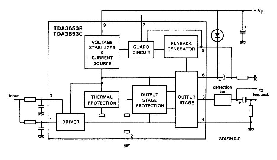
TDA3653B features: (1)Driver; (2)Output stage; (3)Thermal protection and output stage protection; (4)Flyback generator; (5)Voltage stabilizer.; (6)Guard circuit.
Diagrams

| Image | Part No | Mfg | Description |  |
Pricing (USD) |
Quantity | ||||
|---|---|---|---|---|---|---|---|---|---|---|
 |
 TDA3653B |
 Other |
 |
 Data Sheet |
 Negotiable |
|
||||
 |
 TDA3653B/N2,112 |
 NXP Semiconductors |
 Video ICs VERTICLE OUTPUT |
 Data Sheet |
 Negotiable |
|
||||
 |
 TDA3653BU |
 NXP Semiconductors |
 Video ICs VERTICLE OUTPUT |
 Data Sheet |
 Negotiable |
|
||||
 (China (Mainland))


